TFT-LCD array technology
TFT-LCD technology can be divided into array technology, box-forming technology and module technology according to the processing sequence.In this paper, we introduce the first link array process in detail.
The array process is similar to the semiconductor process in which TFT devices, pixels and other patterns are regularly made on a glass substrate.The array process includes a cleaning process, CVD film forming, Sputter film forming, Photoresist or Photoresist (PR) coating, development and stripping, exposure, wet etching, dry etching, etc.Finally, a pattern of 4~5 layers of film is formed on the glass substrate.The pattern formation process of each layer of film is shown in the figure below:
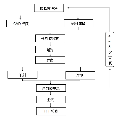
Clean the glass substrate first, then film it (metal Sputter, nonmetal CVD).After the film was made, PR was coated on the substrate and exposed with a MASK.

The pattern needed was transferred from the MASK to PR, and then the photosensitive part in PR was developed and washed, leaving PR as the desired pattern.Then carry out etching (wet etching for general metal, dry etching for non-metal), remove the film without PR protection, and leave the required film pattern.And then you peel off the PR.Annealing treatment is performed at the end of the array process, and the engineering inspection is carried out throughout the array process as required.
The above is a detailed introduction to the array technology of TFT LCD.We hope it will be helpful for you to understand LCD technology.About TFT LCD customization, selection and other questions and requirements, welcome to consult Disea technical staff, we will provide you with the best LCD solutions.